Difference between revisions of "PIN Diode Driver (8-channel)"
m |
(Added notes on switching speed) |
||
| Line 37: | Line 37: | ||
'''Part substitutions''' are possible if some of the specific part numbers used in this design become unavailable. See "0 parts substitution notes.txt" in the design files. | '''Part substitutions''' are possible if some of the specific part numbers used in this design become unavailable. See "0 parts substitution notes.txt" in the design files. | ||
<br />There are inductors in series with each input power lines to serve as '''RF blocks'''; a high-impedance parallel resonant configuration was not possible due to the unexpectedly large/unpredictable parasitic capacitances. However, these still do provide some impedance at 100-300 Mhz. | <br />There are inductors in series with each input power lines to serve as '''RF blocks'''; a high-impedance parallel resonant configuration was not possible due to the unexpectedly large/unpredictable parasitic capacitances. However, these still do provide some impedance at 100-300 Mhz. | ||
| + | '''Switching speed''' is slow, with up to 10µs turn-off time depending on configuration (8µs measured with a single large Macom PIN diode typically used for transmit switching in the RF Lab's coils). Because the Siemens scanner allows ~100µs for the switching to happen, this design is optimized for fairly low parts count, low off-state power, and robust design rather than switching speed. | ||
== Design files == | == Design files == | ||
Design files were created in KiCAD 5 | Design files were created in KiCAD 5 | ||
[[Media:PIN_driver_8x_1.1.1.zip]] | [[Media:PIN_driver_8x_1.1.1.zip]] | ||
Revision as of 18:42, 25 June 2020
Overview
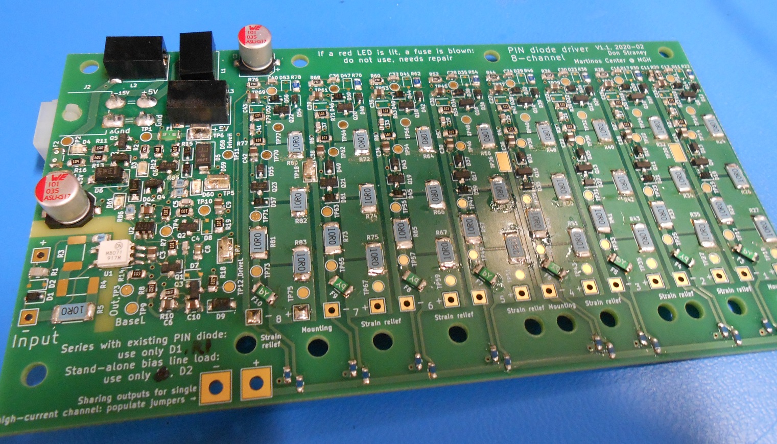
This PIN diode driver is intended to allow new RF coil designs to use more PIN diode channels than the Siemens scanners provide, especially for high-channel-count coil designs. Mounted to an RF coil, it takes on/off input control from an existing PIN diode line from the scanner, and drives the 8 channels in sync with the scanner's PIN diode line.
Using the drivers
Connections and Power
Power inputs are +5V @ 1A (for forward bias), and -15V @ 10 mA (for reverse-bias). Each output provides 100 mA (nominal) when on, and approx. -14.5V when off.
- Protection consists of two SMT fuses, one for +5V and one for -15V, and "resettable" PTC fuses in the reverse-bias drivers.
- The +5V fuse is a Schurter 3413.0219.22, but any 1206-size 2A fast-blow fuse will work. The -15V fuse is a Schurter 3413.0213.22, but any 1206-size 0.2A to 0.5A fast-blow fuse will work.
- A red LED (one for each fuse) will light if power is applied and one of the power input fuses is blown. This can happen due to reversed power supply polarity/incorrect power supply connection, power supply over-voltage, or shorted outputs. The fuses can be de-soldered and new ones soldered in place; it is not worth the extra size/space, risk of eddy currents or image artifacts, etc. to use replaceable fuses as there are few opportunities to blow the fuses through user error once the PIN drivers are incorporated into a permanent setup.
- Do not replace the fuses with solid jumpers! This would likely cause parts to overheat and catch on fire in case of a fault, instead of a safe blown fuse to replace.
Power connections are through a 2x2 Molex Mini-Fit Jr. connector. The pinout for this connector is shown on the top-side PCB silkscreen text next to the connector pins. Input sense connections and PIN driver output connections are through soldered through-hole connections.
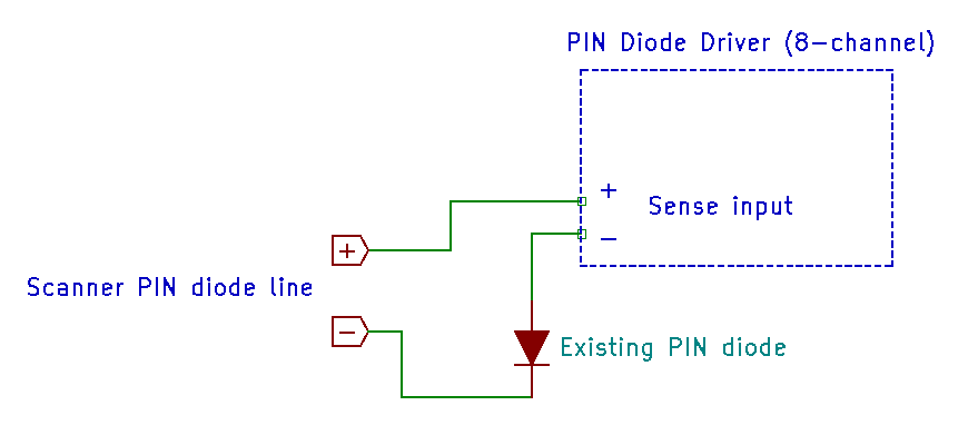
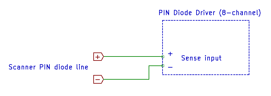
- There are two options for connecting the sense input to a scanner PIN diode line:
- In series with an existing PIN diode: populate D1 and R1, and make sure D2 is removed
- As a stand-alone load on the scanner's line: populate D2, and make sure D1 and R1 are removed
- The sense input is electrically isolated from the rest of the circuitry and so there should be no sense connection concerns with ground loops, etc.
Outputs can be combined into a single 800 mA output, by populating the 16 jumpers (0603-size) along the bottom edge of the PCB, and using the larger output through-hole connections near the bottom-left edge.
Mechanical form factor
See the mechanical drawing here for PCB dimensions, locations of mounting holes, and clearance needed above/below the PCB:
Media:PIN_driver_8x-mech.pdf
The default mounting (as shown in the layout and on the silkscreen) for the Molex Mini-Fit Jr. power connector is on the bottom side of the board. However, if necessary for space constraints, this connector can also be installed on the top side of the board, or it can be left off completely (with wires soldered directly to the through-hole pads).
The PIN driver can operate continuously with all channels on, at full current, without being damaged; however it does generate a reasonable amount of heat, so don't put it inside a closed box. Mounting an insulating sheet of plastic/fiberglass/etc. 10 mm above the top of the PCB is reasonable though, to keep conductive objects and dust from falling on it.
Operation and Modifications
Output current is not regulated, due to the difficulty of heatsinking transistors in-bore. The output current is set by driving the input +5V supply across a known resistance, into a known range of output voltages. The output current is designed to be 100 mA nominal, but will vary from 82 mA (for a 1.2V PIN diode voltage, in series with 10Ω total RF choke resistance) to 127 mA (for a 0.7V PIN diode voltage, no additional series resistance).
- If the output current is higher than desired, the +5V supply can be lowered slightly. The nominal output resistance is 30Ω, so each 0.1V reduction in supply voltage will reduce output current on each channel by ~3.3 mA. Do not reduce supply voltage below 3.3V (limited by FODM8071). Reducing the +5V supply will also make the output current vary more if output voltage changes.
- If the output current is lower than desired, the +5V supply can be increased slightly. Do not increase it beyond +5.4V (limited by FODM8071 optoisolator and logic inverter). Every 0.1V increase in supply voltage will increase output current on each channel by ~3.3 mA.
- Output current can be increased or decreased further by increasing or decreasing the power resistor values on each channel (R24, R26, and R27 on channel 1, etc.). Do not make significant increases to the output current (>120 mA) lightly though! Many parts of the design are based around a 100 mA output current; any changes would need to account for output transistor power dissipation (MMBT2907), output transistor base current and min. beta, output resistor power dissipation and measured steady-state temperature with all channels continuously driving full current.
The reverse-bias voltage has some room for adjustment:
- If a lower reverse bias is desired (down to approx. -6V is possible), reduce R10's value so that it conducts about 3.5 mA or a little more.
- If a higher reverse bias is desired, change or remove the 15V TVS diode D6. The largest limitation on the reverse-bias voltage is the 30V rating of the BAT54H Schottky diodes: in operation they see about 15V+5V=20V. I wouldn't recommend using any more than -20V reverse-bias. If the BAT54H parts are replaced with a similar small-signal Schottky diode with a higher voltage rating, the driver could tolerate up to -30V reverse-bias (limited by the MMBT2222 output transistors).
Part substitutions are possible if some of the specific part numbers used in this design become unavailable. See "0 parts substitution notes.txt" in the design files.
There are inductors in series with each input power lines to serve as RF blocks; a high-impedance parallel resonant configuration was not possible due to the unexpectedly large/unpredictable parasitic capacitances. However, these still do provide some impedance at 100-300 Mhz.
Switching speed is slow, with up to 10µs turn-off time depending on configuration (8µs measured with a single large Macom PIN diode typically used for transmit switching in the RF Lab's coils). Because the Siemens scanner allows ~100µs for the switching to happen, this design is optimized for fairly low parts count, low off-state power, and robust design rather than switching speed.
Design files
Design files were created in KiCAD 5 Media:PIN_driver_8x_1.1.1.zip


